
As I announced to my newsletter subscribers, I knew I was going to be busier than usual participating in the Meshtastic Build-Off 2026 competition. Rather than leaving the blog without new posts in the meantime, and because I think this can be a genuinely interesting series, I decided to write about parts of this process so you can follow along with the development of a device from PCB to firmware integration. Though in this case, the firmware side will be a bit different from the usual, since the goal is to get my new hardware running with Meshtastic’s existing firmware.
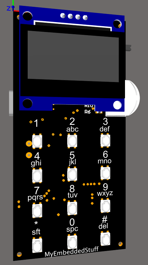
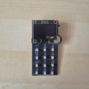
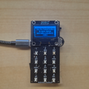
The device I’m building is called the RetroMeshDevice. The idea was to build a companion node that is as minimal as possible and doesn’t depend on a phone to send messages. There are already some very polished options on the market — QWERTY keyboards, touchscreens, the works. Fair warning: I’m not going to match any of that. The competition runs for a few months, and the goal is to build something fun, functional, and useful. So to give it a different feel from what I’d already seen out there, I decided to go retro: a small OLED display and a T9-style keypad as the main input method, just like old mobile phones. Compact enough to carry, but capable of operating independently without needing a phone connection.
If you want to stay up to date on this build and the upcoming posts in this series, I’d recommend subscribing to the newsletter. I’ll be sending updates a few days before each new post goes live.
In this post I’ll go through the first part I’ve worked on: the PCB, focusing on the schematic and the reasoning behind each design decision.
I’ve tried to structure the most important sections around the key components that make up this board.
Table of Contents
ToggleMicrocontroller
The component that will run the Meshtastic firmware is the XIAO ESP32-S3 Plus from Seeed Studio. I chose it because I’m already familiar with ESP32 modules, which would make the Meshtastic integration straightforward.
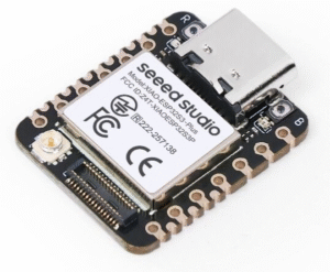
On top of that, XIAO modules offer a lot for their price: they pack a USB-C connector and a battery charging circuit into a small footprint. That meant I could have the charging and USB connectivity sorted on my PCB, already designed, already tested, for a very small cost difference, without having to design any of that from scratch.
I have a short post where I talk about them and their relationship with Zephyr, if you’re interested:
https://myembeddedstuff.com/how-to-flash-zephyr-rtos-on-windows-xiao-boards
As for why the ESP32-S3 Plus specifically: pin count. The standard ESP32-S3 was too limiting for what I had in mind. The radio module alone — which I’ll cover in the next section — already takes four GPIOs for the SPI interface (MOSI, MISO, SCK, NSS), plus additional lines for BUSY, DIO1, RST and RF_SW. Add the I2C lines needed for a display and the pin count climbs fast.
In my configuration, the microcontroller defaults to reset state to minimise current draw. I wanted to make sure the device can still charge the battery over USB while powered off, and that off-state consumption stays as low as possible. When the slide switch is flipped to ON, the microcontroller will boot. This is covered in more detail in a later section.
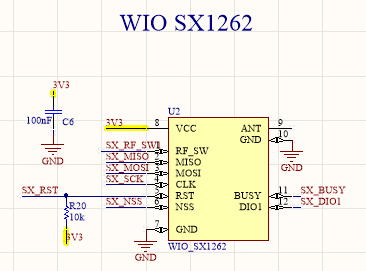
Radio module: WIO SX1262
The radio module I went with is the WIO SX1262. The competition rules allowed up to three different options, but I had already seen several builds using the WIO SX1262, it was familiar territory, and it was also the most affordable of the three — which always matters in a maker project, since building in small quantities is expensive enough as it is.
The SX1262 is a solid choice for this kind of project: it supports the 868 MHz band, has excellent sensitivity, and handles all the LoRa modulation in hardware, the MCU just needs to send and receive packets over SPI.
The wiring follows the standard SX1262 SPI interface: MOSI; MISO, SCK and NSS as chip select, plus the dedicated lines BUSY, DIO1, RST and RF_SW. That last one, is important and easy to overlook. The SX1262 needs that signal to switch the RF path between TX and RX. If it isn’t handled correctly in firmware, you end up with a radio that either receives but won’t transmit, or transmits but won’t receive a classic mistake on first designs with this chip.
The SX_BUSY line is equally critical: the SX1262 uses it to tell the MCU it’s still processing a command. If you kick off a new SPI transaction while BUSY is high, you corrupt the radio’s internal state. You always need to wait for BUSY to go low before talking to the chip again.
Battery Measurement Circuit
Reading battery voltage with an ADC is straightforward in principle — a resistor divider, two resistors. But there’s a catch: if you leave the divider permanently connected, it drains the battery continuously, even if slowly. On a device built to last, that’s wasted energy. Beyond making the battery discharge faster, it also means that if you leave the device in a drawer with the battery installed, it will keep draining down to a voltage level that can actually damage the cell.
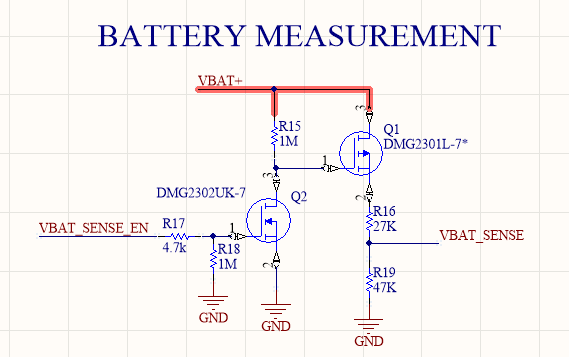
The solution here uses a MOSFET (DMG2302UK) as a switch controlled by the VBAT_SENSE_EN signal from the ESP32-S3 Plus. When the firmware needs to read the battery level (VBAT_SENSE), it asserts the enable pin, the MOSFET connects the divider, waits a few milliseconds for the signal to settle, takes the ADC reading, and then turns the MOSFET off again. The divider is only active for milliseconds at a time.
The resistor values are chosen to bring the VBAT+ voltage down to a safe level for the ESP32-S3 Plus ADC, which has a maximum input of 3.3V. With R_top at 27K and R_bottom at 47K, the divider ratio is 0.635. The three relevant scenarios:
| Condition | Input V | ADC V |
|---|---|---|
| LiPo Empty (3.2V) | 3.2V | ~2.03V |
| LiPo Full (4.2V) | 4.2V | ~2.67V |
| Absolute Max (5V) | 5.0V | ~3.17V |
In all cases the output stays below the 3.3V ADC limit, with a safety margin even in the worst-case scenario.
Keypad: 4×3 Matrix via MCP23017
The keypad is a 4×3 matrix in phone layout — twelve keys covering 0 through 9 plus * and # enabling T9 text input for sending messages over the mesh. Twelve keys, and rather than spending 12 GPIO pins on the ESP32-S3 Plus, I’ve routed it through an MCP23017 I2C GPIO expander.
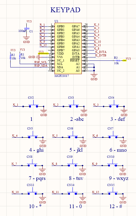
The MCP23017 provides 16 bidirectional GPIO pins over I2C and only needs 2 lines from the MCU (SDA + SCL). It also has two interrupt outputs (INTA and INTB), which I’ve wired back to the ESP32-S3 Plus. When any key is pressed, the MCP23017 notifies the MCU immediately rather than requiring constant polling. This is much better for the microcontroller, which can be busy handling other tasks without caring about the keypad at all until the interrupt fires.
The MCP23017 also has a particularly useful feature: you can configure the GPA and GPB pins with internal pull-ups, which saves us from placing pull-up resistors on the PCB for each key line.
The pull-up resistors on SDA and SCL (10K) are mandatory for I2C to work correctly. I chose that value because, being on the higher end of the resistance range, the current draw through them will be slightly lower, every µA counts. It could in theory affect signal integrity, but at the frequencies we’ll be running at I don’t expect it to be an issue.
Power supply: TPS79533 regulator
The main regulator is a TPS79533DCQR, a low-dropout LDO from Texas Instruments that outputs a clean 3.3V. I picked this part for a few reasons beyond just “it outputs 3.3V”:
It has very low quiescent current, which matters for a battery-powered device, and the noise performance is good, it’s a low-noise LDO, which is important when you have an RF radio on the same rail.
The input (VBAT+) comes directly from the battery, and I have decoupling caps on both the input and output rails. The 3V3 net feeds the ESP32-S3, the SX1262, the display, the keypad IC, and everything else. One clean rail for everything keeps the design simple.
Here’s a breakdown of the components it powers:
| Component | Conditions | Typical Current | Peak Current |
|---|---|---|---|
| WIO SX1262 | RX active / TX @ +22 dBm | ~5 mA | ~120 mA |
| Display OLED | SSD1306 | ~15 mA | ~25 mA |
| Keypad Expander | MCP23017 normal op. | ~1 mA | ~2 mA |
| Pull-ups & Misc | I2C, encoder, divider | ~2 mA | ~5 mA |
| Total Estimated | All systems active | ~23 mA | ~152 mA |
I’ve sized the regulator at 500 mA to give plenty of headroom, running a regulator close to its limit is never a good idea. That said, a 300 mA part would have covered this design just fine.
Power-On Circuit
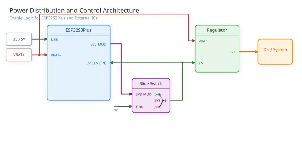
Input power arrives either from the battery (VBAT+) or via USB, both feeding directly into the XIAO ESP32-S3 Plus. The XIAO exposes a 3V3_MOD rail on its 3.3V output pin — this rail is always live as long as the XIAO itself is powered.
From 3V3_MOD, the signal passes through a user-accessible slide switch. When the switch is open, the ESP32-S3 Plus EN pin is not asserted and the TPS79533 is not enabled — the device is fully off. When the switch is closed, 3V3_MOD drives the 3V3_EN node, which connects to both the EN pin of the TPS79533 LDO regulator and the EN pad of the XIAO ESP32-S3 Plus, bringing the microcontroller out of reset and enabling the regulator simultaneously.
Once the TPS79533 EN pin is asserted, it takes VBAT as its input and outputs a clean 3V3 rail. This regulated supply feeds all the downstream ICs: the SX1262 LoRa transceiver, the SSD1306 OLED display, and the MCP23017 I/O expander.
Conclusions
I’ve tried to walk through the main components so the reasoning behind each decision is clear. That said, I haven’t covered everything, there are a few elements in the design I’m keeping back for later, so there will be some surprises along the way.
If you don’t want to miss any part of this series, I’d recommend subscribing to the newsletter, where I usually share updates a few days before each post goes live.
And if you have any questions about the schematic, something that wasn’t clear, or just want to leave a comment, the comments section is below for that, or you can reach me through the contact page. I’d also love to know if you enjoyed this kind of in-depth technical content and want to see more of it.
I’ll share the full schematic later on, once everything has been validated against the real hardware. I don’t want to publish something that might need corrections.
Thanks for sharing your progress. I am a long time radio nerd so I do enjoy the technical guts of a project. Far as your design goes I totally love the form factor. That T9 entry brings back some fond Nokia candy bar phone memories. The snap on face plates were the coolest things.
But If you decide to manufacture some of these I would love to buy one.
Thank you, Katherine, for your kind words; I’m glad you liked it. I will keep writing more posts, so if you want to subscribe to the newsletter, you can stay updated on new content.
Regarding the commercialization, I’ve noted your email and will let you know once the design is finished. I imagine I will decide to send out some boards if people are interested. Once the firmware is done and everything is tested, I’ll keep you posted. Best regards.
Pingback: Meshtastic Build-Off 2026: PCB Assembly - myembeddedstuff.com
Pingback: Meshtastic Build-Off 2026: Hardware Bring-up and Initial Validation - myembeddedstuff.com
Pingback: Build off 2026 - Meshtastic firmware implementation - myembeddedstuff.com